Hacking an NFC ring
by ecotner on Wed Aug 30 07:40:28 2023
Tags: #hardware, #hacking, #electronics,
A couple weeks ago, I was exploring downtown San Diego during Comic Con 2023 with some buddies. None of us actually had tickets so we were just hanging around outside the convention center, which is still pretty cool because of the masses of people wandering around dressed up like characters from their favorite comics, video games, movies, shows, etc.
There are also lots of exhibits and shows in the area around the center where studios are teasing their upcoming series and giving away swag. We happened to walk into the FX area where there was an "immersive experience" to hype up their new series "A Murder At The End Of The World", hidden within an inflatable white dome. The wait in line was about an hour, but the sign promised jump scares so we decided to tough it out in hopes of something exciting. It turned out to be a major letdown; they had us sit in a mock airplane cabin while a creepy flight attendant pretended we were VIP guests of one of the characters from the show (an uber-rich philanthropist) for a couple minutes, then led us into another room designed to look like an (ant?)arctic wasteland and showed us the trailer for the show... and that was it. I'm still not even sure what the jump scare was supposed to be! The trailer volume was kind of loud so maybe it had something to do with that?
Anyway, what does this have to do with NFC? Well, during the airplane cabin part they gave us some plastic rings that had embedded NFC tags that would take you to https://www.fx.tv/SmartRing.
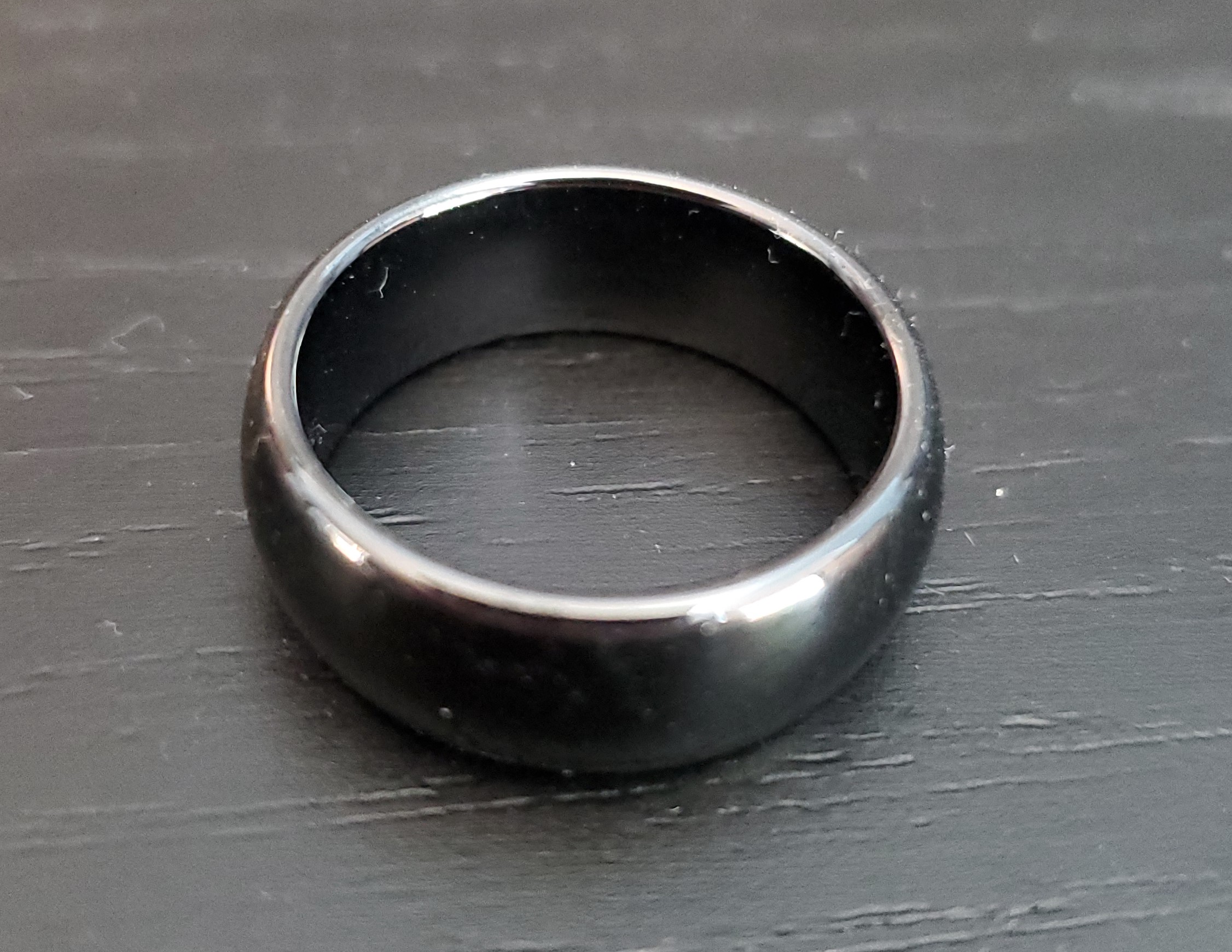
I thought that was pretty cool and started wondering if it was possible to reprogram the ring's chip to put some custom data on it. Maybe a link to my website/blog or some kind of funny image?
So this is basically the story of how I spent the next couple of days going down the rabbit hole of NFC in an attempt to hack this ring.
What is NFC?
First off, let's start with what NFC is at a high level. NFC stands for "Near Field Communication", which makes sense if you've ever used the NFC capability on your phone before; you need to be near the device you're communicating with in order for it to work. It turns out that NFC is a special subtype of another common technology you've probably heard of before called RFID (Radio Frequency ID). RFID encompasses quite a few different communication methods. These devices can be either active (has a power source of its own, typically to increase range) or passive (has no power source and must be "interrogated" by another device using electromagnetic induction), and communication can be either 1-way (e.g. a tag with a static data payload that is written once when the tag is created and read from later) or 2-way (e.g. information can be both read from and written to the tag repeatably). It can also typically operate at three different radio frequencies: low-frequency( 125 kHz), high-frequency (13.56 MHz), and ultrahigh-frequency (860-956 MHz). The hardware communication protocol used by RFID (generally called "proximity cards") is outlined in ISO 14443-3.
NFC is therefore the specific subset of RFID where
- the tag is passive and must be interrogated by another device, limiting range of operation to several centimeters
- communication is 2-way; information can (in principle) be read from and written to the tag device
- operates in the high-frequency band, which can easily be generated by mobile phone sized antennae
- has some higher-level communications protocol standardized by the "NFC Forum"
I personally wasn't really sure what the difference was at first, but a quick web search turned up plenty of articles with this information.
Write-locked tags
What was a little more difficult to find though was information on how to actually write to an NFC tag. I came across some old forum thread (can't find the link at the moment!) that explained that any old mobile phone would have this capability and suggested downloading an app that could do this for you. After doing a quick review of several apps, I installed NFC Tools for android since it seemed to be the most popular. This tool has both the ability to read and write, along with some more advanced features that would come in handy later. Upon first scanning the tag, I was shown a variety of useful bits of (meta)data and attributes:
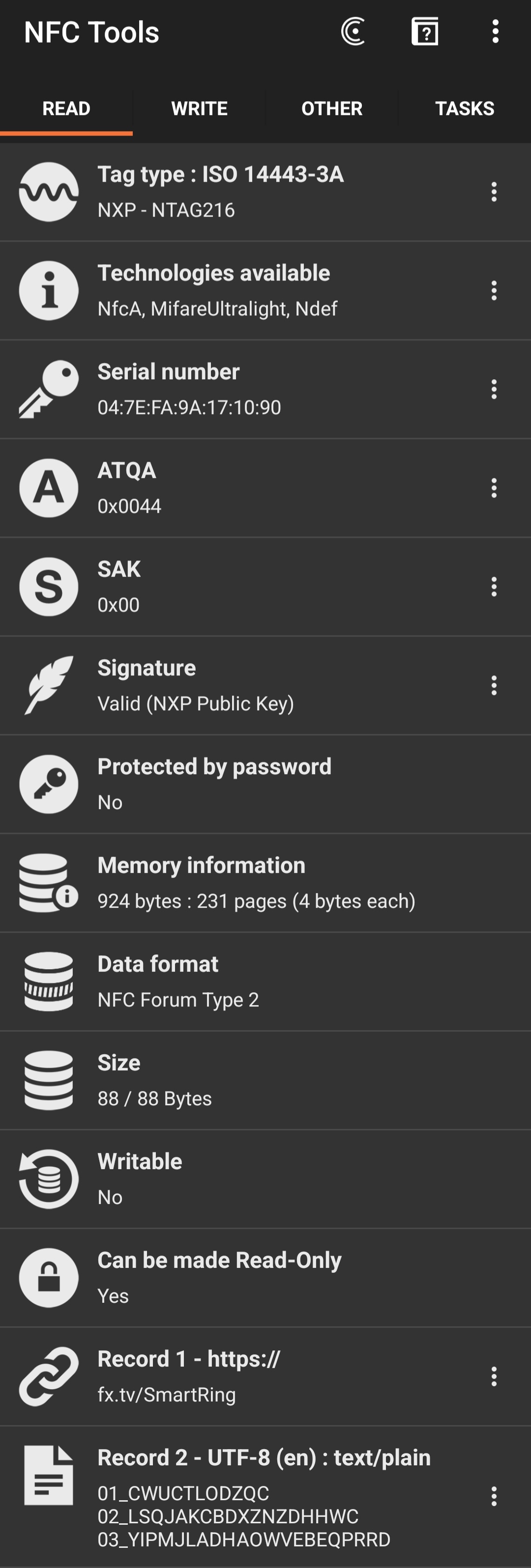
A couple things that immediately jumped out at me:
- memory was only about 1 kB (88 bytes under "size" + 924 bytes under "memory information" = 1012 bytes)! I guess this makes sense; these tags are supposed to be just big enough to hold a URL or a contact card, not HD videos
- the tag actually contained two records
- the aforementioned URL https://fx.tv/SmartRing
- plain text data that looked like some kind of ID numbers? (
01_CWUCTLODZQC,02_LSQJAKCBDXZNZDHHWC, and03_YIPMJLADHAOWVEBEQPRRD)
- a field that said "Writeable: No" :'(
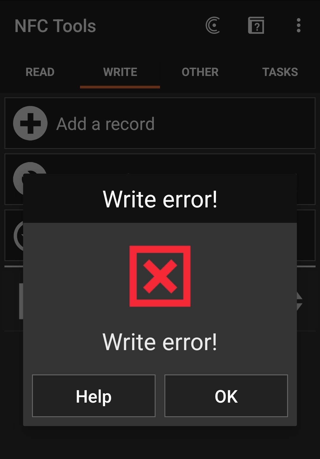
That last item was a little concerning. Was this basically a lost cause? Could I not overwrite the data on this tag? A quick attempt to write some random text to the tag was met with an unfortunate write error message.
I was dismayed, but decided to keep searching online to see if there was any workaround. Various sources I found suggested that either it was impossible unless you had the original device that "locked" the tag initially (looking back, this might have been a reference to password-protected tags, but after researching this further there doesn't appear to be any write-device-level locking), or locking is permanent and cannot be reversed (this is actually true).
I was ready to give up, but then suddenly stumbled upon this stackoverflow post that blew the case wide open. Apparently the write-locking mechanism is not globally applied to the entire memory, but just specific "pages" according to specific lock bits (which are permanent once set unfortunately). From the tag metadata, it looked like I had 231 pages to play around with, so maybe there was some section of the memory that wasn't locked I could modify. The author of that answer miraculously mentioned the exact type of NFC chip that my ring used (the NTAG216 from NXP), and suggested looking up the data sheet for more information about the memory layout and locking mechanism, so that's exactly what I did.
Hardware of the NTAG216 and memory layout
I pretty easily found the data sheet for the NTAG216 after a quick search. A quick scan of the document revealed section 8.5 (Memory organization) as a prime target for investigation. Like the SO post said, the memory was arranged in 231 "pages", which were each composed of 4 bytes. (In what follows, I'll refer to numbers in hexidecimal using the prefix '0x', and binary with '0b'. A lot of the NFC documentation refers to hex values using the postfix 'h' though, so don't get confused. For example, 0xA = Ah = 0b1100 = 10.)
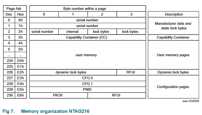
The first couple of pages contained some metadata about the chip like its serial number and "capability container" (more information about how the memory is laid out from what I can tell), but also two "lock bytes" in page 0x02 which looked relevant. Then were about 220 pages of "user memory" which I assumed was the location of the actual data we would want to put on the chip, followed by a couple more pages with some configuration data, password protection stuff, and finally 3 "dynamic lock bytes" in page 0xE2. The bytes labeled RFUI are "Reserved for Future Use - Implemented", which I think basically means "don't use this space".
The first set of lock bytes were known as "static" lock bytes, where basically each bit in the two octets represented a lock on one of the pages in the user memory section.
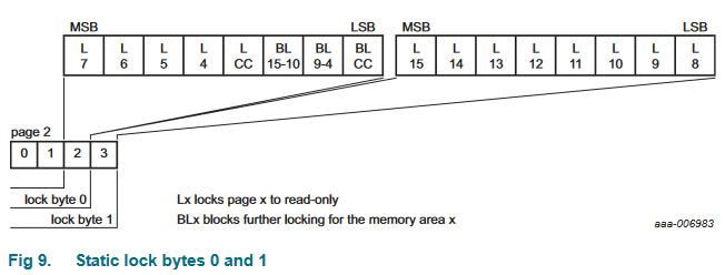
There are only 16 bits in two bytes though, so that means you could only lock 16 pages maximum, way fewer than there actually were available. Some of the other bits would actually block small page ranges from locking if you wanted to prevent someone from making certain memory sections write-only.
The dynamic lock bytes appeared a little more powerful, if more coarse-grained.
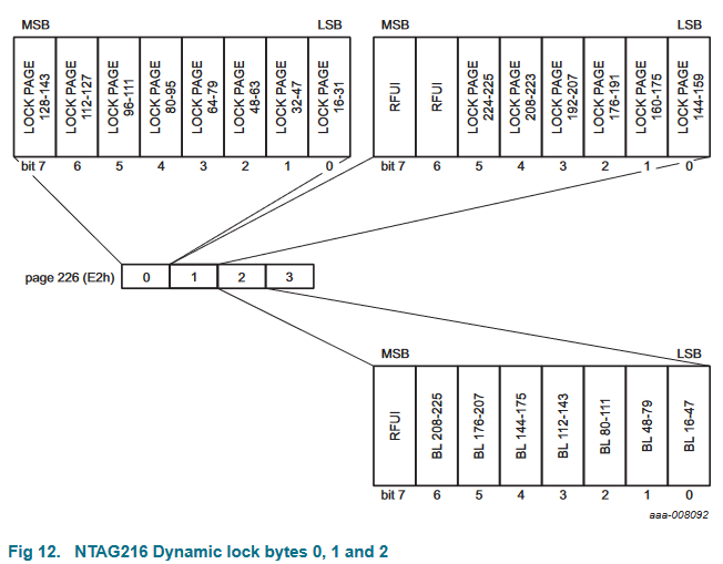
Each bit in the first two bytes represented 16-page blocks, and the third byte contained blocks on 32-page ranges.
Ok, so now that we know what the locking bits do, where they are, and which user memory pages they are applicable to, the next thing to do was actually check the data on the chip to see how these bits were set.
The NFC Tools app has an "other" tab with a "read memory" functionality we can use to inspect the raw data in the individual pages.
Running this on the tag revealed that the two static locking bytes both had values 0xFF = 0b11111111 (i.e. every bit was enabled so all pages between 0x03 and 0x0F were locked), but the dynamic lock bits were all disabled (the bytes set to 0x00).
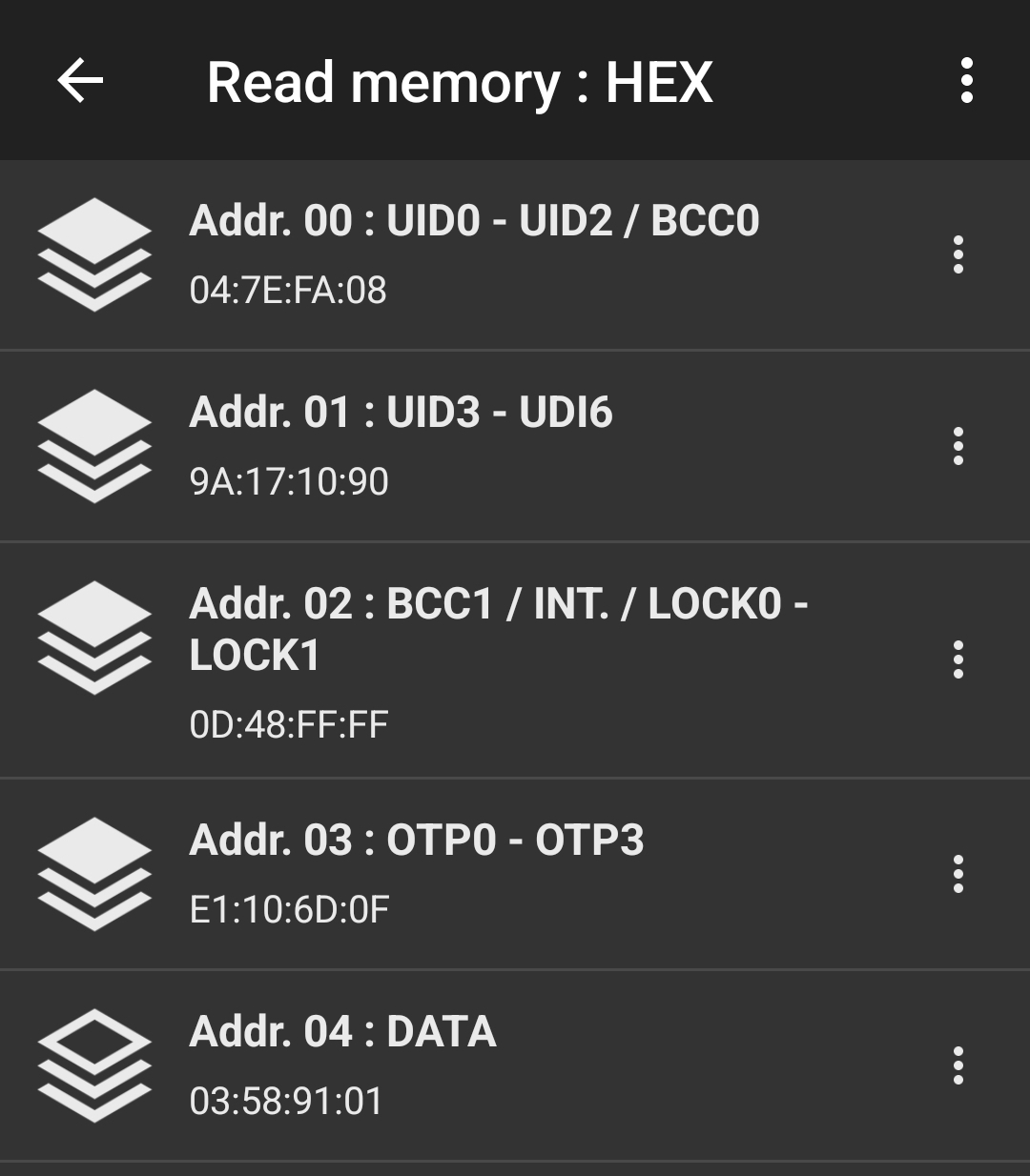
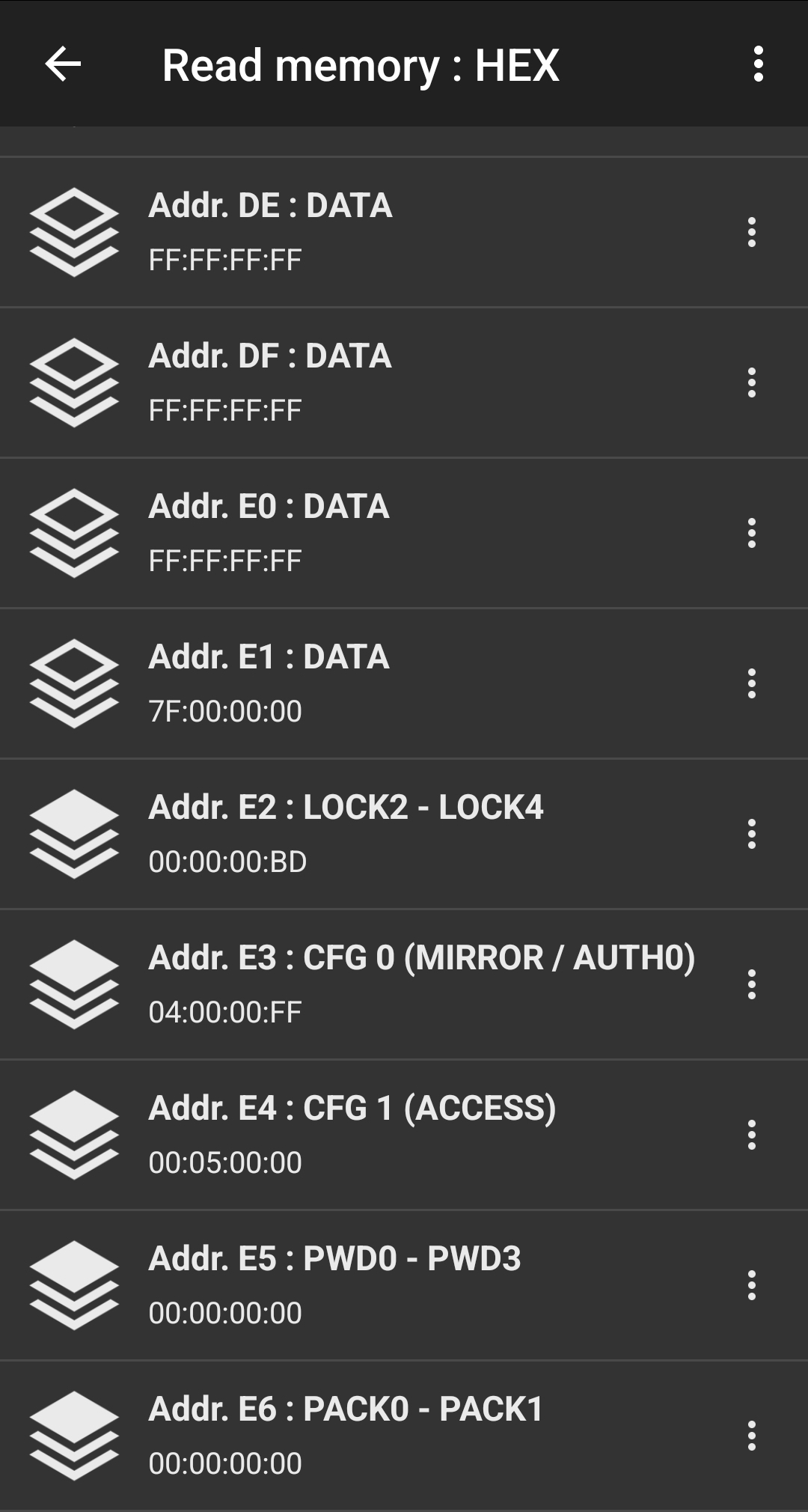
So even though the first dozen or so pages of user memory were locked, the vast majority of them weren't! But if that was the case, then why was NFC Tools saying the whole chip was locked? And if those pages really were unlocked, how could I write to them?
Manual bit manipulation
The solution to this problem came to me as most good solutions do, while I was fucking around with something I shouldn't have been. Under the NFC Tools' "other" tab is a menu item called "Advanced NFC Commands". When you tap this, a very scary warning pops up to say you should not be messing around with this tool unless you know what you're doing, and it is quite possible you may brick your NFC device.
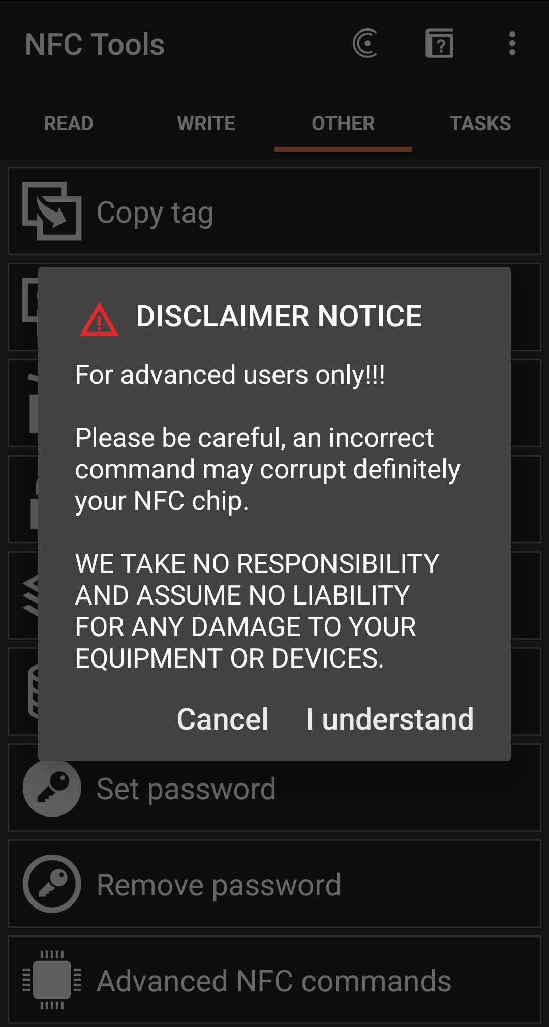
Obviously I immediately hit the "I understand" confirmation, and was presented with a menu that appeared to allow you to send commands to a tag with some kind of data payload attached.
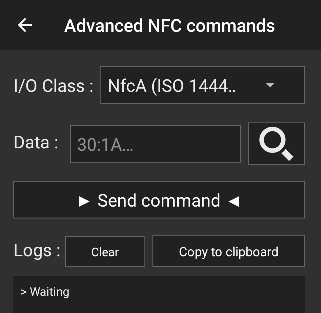
The I/O field obviously specified the tag communication protocol from ISO 14443 (of which this device was Type A as it said in the metadata from earlier), but I wasn't sure how to specify commands, what commands were even available, or what the data field was for. This prompted me to start looking for NFC commands. In the NTAG216 data sheet under sections 9 (Command overview) and 10 (NTAG commands), I was able to find low-level descriptions of available commands and how to format them correctly. The data field has a special prefix byte that indicates which command you want to send, (potentially) followed by additional bytes that provide arguments to the command.
The GET_VERSION command, for example, is specified by the prefix byte 0x60, and requires no arguments.
When I send this command to the NFC device, I get the following response:
00:04:04:02:01:00:13:03
which turns out to represent a bunch of product information like vendor, product (sub)type and version, storage size and protocol.
There is also a WRITE command, which is prefixed with 0xA2, followed by one byte representing the page address you want to write to, and 4 more bytes representing the data to be written.
For example, the command A2:04:DE:AD:BE:EF will write the data 0xDEADBEEF to the page 0x04.
It turns out that because of the static lock bits, this operation will fail because page 0x04 is read-only, but if we were to attempt to write something to a page outside the locked sector (e.g. page 0x20), this succeeds (the response byte 0x0A represents an ACK, which is decribed in section 9.3 of the NTAG data sheet)!
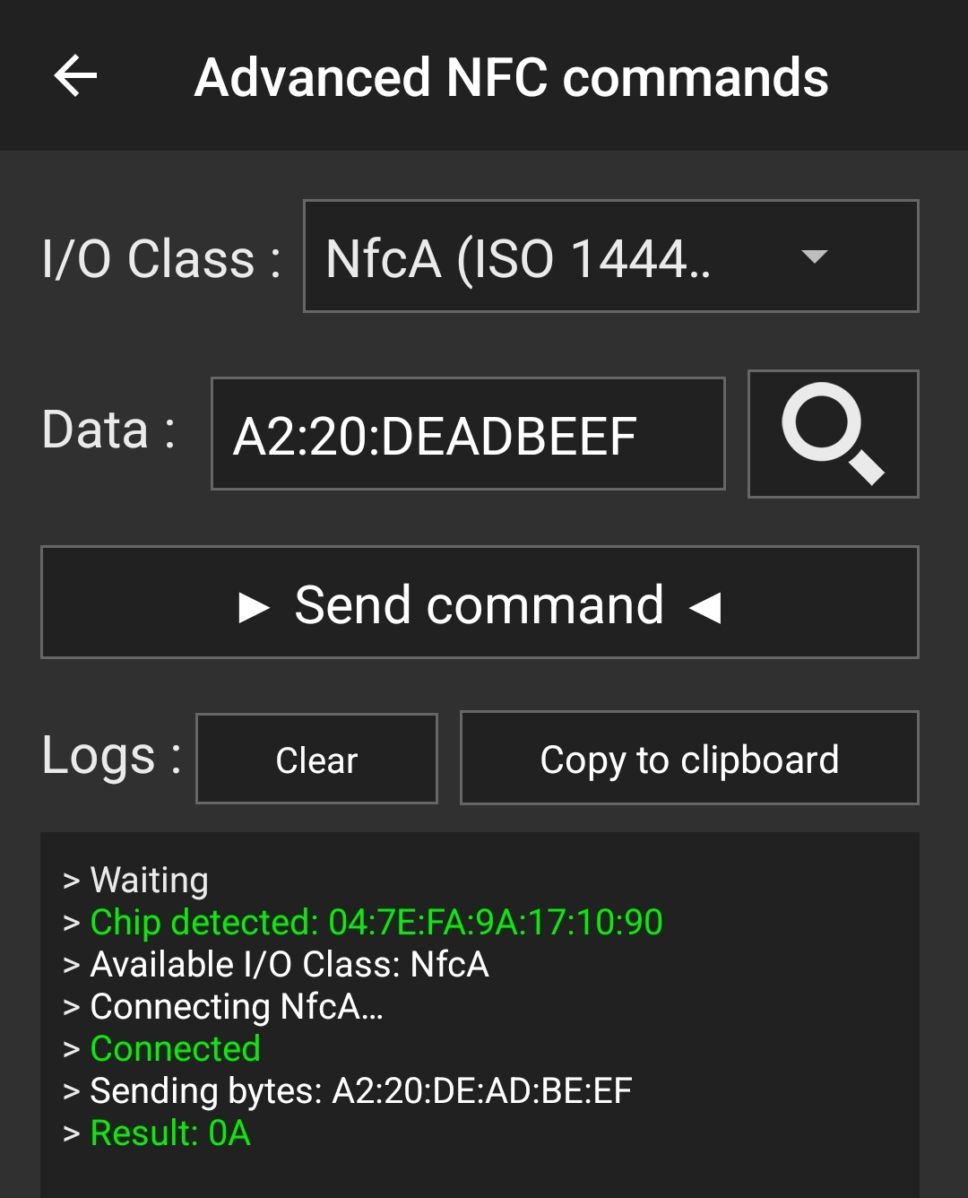
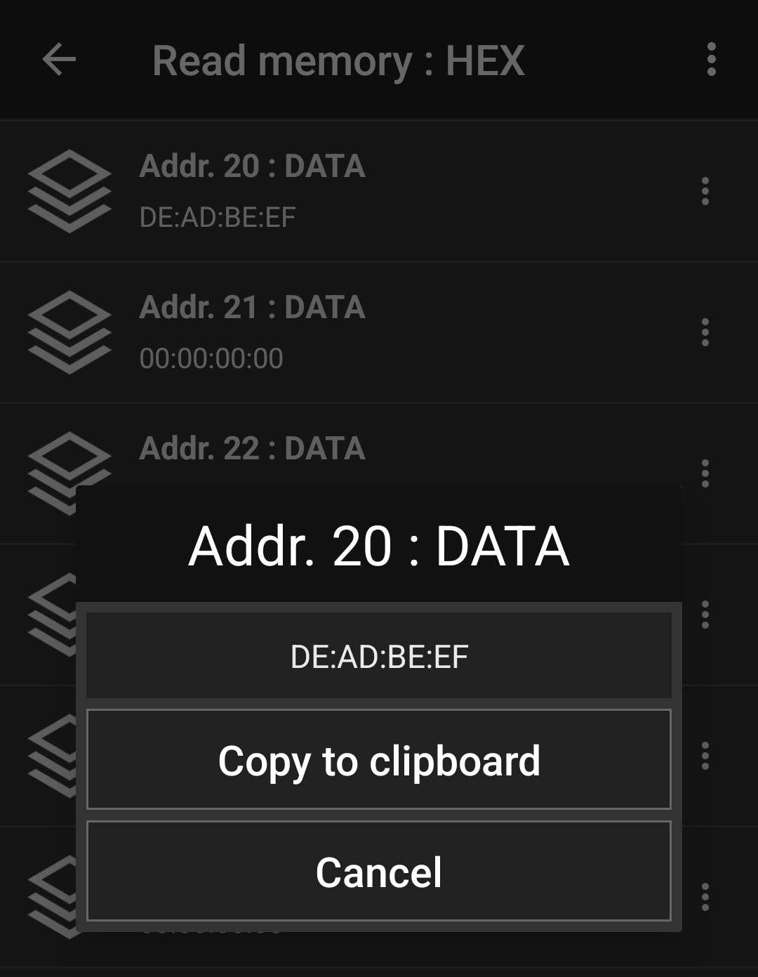
So we can actually write to the NFC tag in the unlocked sector! But does this mean we can put some information on there that can be used in a practical way?
NDEF message format
In order to put useful information on the NFC tag, we need to know how that data needs to be formatted so it can be read and parsed properly by other applications. We obviously can't just throw any old bytes into random pages and expect our phone to be able to interpret them correctly. The NTAG data sheet unfortunately does not have anything to say about data formats because that is considered a higher level of abstraction.
It turns out the correct data structure is called NDEF (NFC Data Exchange Format), which is specified by an international standard put together by the "NFC Forum". At a high level, this data structure is composed "NDEF messages", and each message is composed of sequential "NDEF records" which each have their own specific types and can represent any arbitrary chunk of data like a URL, image, text, or binary blob. NDEF records have a header which at its bare minimum contains information about the record type and payload length, but also allows for an optional ID, chunking, and flags to indicate the beginning/end of the NDEF message. Following the header is the data payload itself.
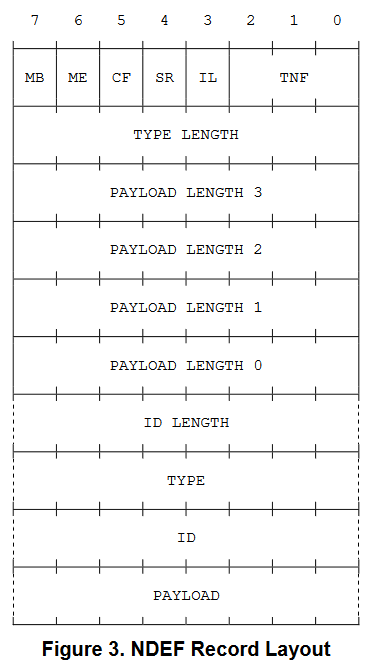
A simple example of a complete NDEF message containing two text records each saying "hello" and "world" would be
91:01:05:54:68:65:6C:6C:6F // first record "hello"
51:01:05:54:77:6F:72:6C:64 // second record "world"
where
- 0x91 = 0b10010001; i.e. header of the first record of the message (MB=1), single payload length byte (SR=1), and type is an NFC Forum well-known type (TNF=0b001)
- because the ME, CF, and IL bits are not set, we know that this record is not the last, is not chunked, and has no ID fields
- 0x01 = 1; i.e. the record type is a single byte
- 0x05 = 5; i.e. the payload is composed of 5 bytes
- 0x54 = "T"; i.e. the payload type is plain text
- 68:65:6C:6C:6F; i.e. the payload is the ASCII string "hello"
- 0x51 = 0b01010001; i.e header of the last record of the message (ME=1), single payload length byte (SR=1), and type is an NFC Forum well-known type (TNF=0b001)
- 0x01 = 1; i.e. the record type is a single byte
- 0x05 = 5; i.e. the payload is composed of 5 bytes
- 0x54 = "T"; i.e. the payload type is plain text
- 77:6F:72:6C:64; i.e. the payload is the ASCII string "world"
Armed with the knowledge of what NDEF messages/records look like, we can inspect the content of the user memory sector of our NFC tag to confirm that it follows this standard. However, it turns out that things don't line up exactly as we'd expect...
NFC Forum Types 1, 2, 3, ... oh my!
If I take a look at the first couple pages of user memory on the chip it looks something like this:
page    bytes           chars
----------------------------------------
0x04    03:58:91:01     \x03 X \x91 \x01
0x05    10:55:04:66     \x10 U \x04 f
0x06    78:2E:74:76     x . t v
...     ...             ...
Ignoring the first two bytes for now, we can see the 0x91 and 0x01 in page 0x04 represent parts of the NDEF header for the first record: 0x91=0b10010001 means MB=1, SR=1, and TNF=1, and 0x01 means the type is of length 1.
In the second page, 0x10=16 is the payload length, 0x55='U' is the record type (short for urn:nfc:wkt:U, i.e. a URI), and all the other bytes represent the data in the first record , which we can see begins with the URL fx.tv... (the 0x04 before the 'f' is a "URI prefix" that represents https://).
So what are the first two bytes 0x03 and 0x58 that precede the NDEF message? Well, it turns out that there is one additional protocol that sits between NDEF and the hardware of the chip, which is known as the "NFC Forum Type". This protocol allows the chip to translate between the raw layout of the user memory sector and the NDEF message(s) contained therein. Our NTAG216 chip is a "Type 2" tag (apparently set by the "capability container" - page 0x03), which means that it has a flat memory structure (other types apparently have an actual file system like Type 4). I was able to find a link to a copy of the Type 2 official spec in a SO post, but the link is dead. It was fortunately archived using the wayback machine though so we can still access it. The relevant section is 2.3: "TLV blocks".
This spec defines a "wrapper" data structure for an NDEF message called a TLV block, where TLV stands for "Tag, Length, Value". Basically what it means is that each block of data in the user memory sector needs to be prefixed by a "tag" byte which indicates the type of data in the block (0x03 corresponds to "NDEF Message", duh), followed by at least 1 but up to 3 bytes representing an integer indicating the number of bytes of data in the block (0x58=88 in decimal so there are 88 characters in the NDEF message, which includes both records). Finally, once all the TLV blocks have been specified (because you can have multiple), you need a "terminator block", which is simply the magic byte 0xFE. If we scroll further down the list of pages, we eventually see that in page 0x1A there is a 0xFE byte, after which the user memory bytes are all set to 0x00 for the rest of the sector, so this is clearly the terminator.
Ok, so all we need to do is wrap an NDEF message in a TLV block and we're good to go!
The ugly reality of the situation
At this point, if the chip had been completely unlocked, we would now know everything we need in order to store any kind of data we want on it. But it isn't unlocked; recall that the lock bits were set to 0xFFFF, meaning pages 0x03 through 0x0F are read-only. This poses several different problems:
- The tag/length headers of the TLV block are in page 0x03, which means that we can't modify the length of the data in the block, meaning any modifications we make to the NDEF message have to preserve byte length
- The first NDEF record is completely within the read-only area (pages 0x04-0x09), so we can't modify it at all
- The header of the second NDEF record is completely within the read-only area (pages 0x09-0x0A), so while we can modify some of its data in pages 0x10 or greater, we can't change its type or length
Well, if the TLV block is basically immutable (at least without corrupting the NDEF message), could we just make a second TLV block and store a second NDEF message in there? Sure, we absolutely can! We just need to remove the TLV terminator byte from page 0x1A (which is outside the locked sector), start the header of our new TLV block in its place, then put the terminator back at the end, and viola! Let's take that example "hello world" NDEF message from earlier and wrap it in a TLV block with header 03:12 (0x03=NDEF message, 0x12=18 bytes of data), using the NTAG WRITE command we discovered earlier:
A2:1A:52:44:03:12
A2:1B:91:01:05:54
A2:1C:68:65:6C:6C
A2:1D:6F:51:01:05
A2:1E:54:77:6F:72
A2:1F:6C:64:FE:00
The first/last commands are a little special. In the first, we write (0xA2) to page 0x1A where first two data bytes 0x5244 are the last bytes of the first TLV bock, and the final bytes 0x0312 are the header of the second TLV block we're creating. The final command writes the final bits of data in the second record (the "ld" of "world"), followed by the TLV terminator 0xFE and a null byte 0x00.
Now let's read the data on the chip back using NFC Tools! Looking at the raw bytes in each individual page, we can see the changes were successful, but when I try to read back the data using the normal scan (which I assume parses the NDEF message), nothing has changed, and we still only see the first message. After some internet searching, I found that android is not capable of recognizing multiple NDEF messages; only the first is read and all subsequent ones are discarded (one person even tried the exact same "2 TLV blocks" method we did, but with no success). iOS apparently has support for multiple NDEF messages (as seen in this example), but I do not have an iPhone so cannot test this, and according to some reddit post, only the first URL record will produce an action by default.
So what now?
It seemed a little depressing to have come this far and learned so much about NFC only to figure out that hacking this ring was impossible, especially because the only thing preventing this was a couple (lock) bits on the chip were 1's instead of 0's. But I started this project with the goal of putting some actionable data an NFC ring, and by god that's what I'm going to do!
If you look for NFC rings online, a number of results pop up with a dizzying range of prices. I saw everything from $500 state of the art chargeable titanium multi-tool rings with NFC+bluetooth support plus heart rate, oxygen, acceleration and temperature sensors, all the way to $0.90 ones on Amazon that have product descriptions clearly written by someone who has no idea what NFC even is (I saw a lot of descriptions that confused NFC with bluetooth) and half the reviews say the product doesn't work.
So I bought about 6 of the $0.90 ones because I figured there was a good chance at least one of them would work (\(1 - (1-p)^n\) where \(p\) is the probability of success and \(n\) is the number of rings, e.g. 98.4% chance with \(p=0.5\) and \(n=6\)).
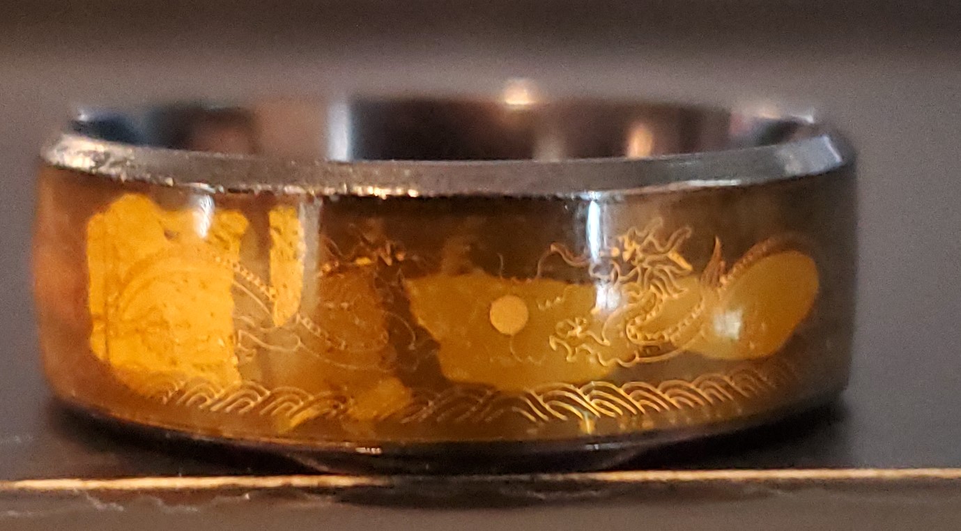
After about a month of waiting for the rings to ship from China, they finally arrived. I got a couple different colors (gold, rose gold, silver, black) for a bit of variety, and they actually look surprisingly nice given the price. The NFC tag/chip is clearly visible as a black rectangle on one side of the ring, protected under a layer of orange epoxy. It is also a bit difficult to make out in the pictures, but there are also images of dragons engraved into the side on each one which is kinda cool (they're only really visible on the black rings because of the contrast).
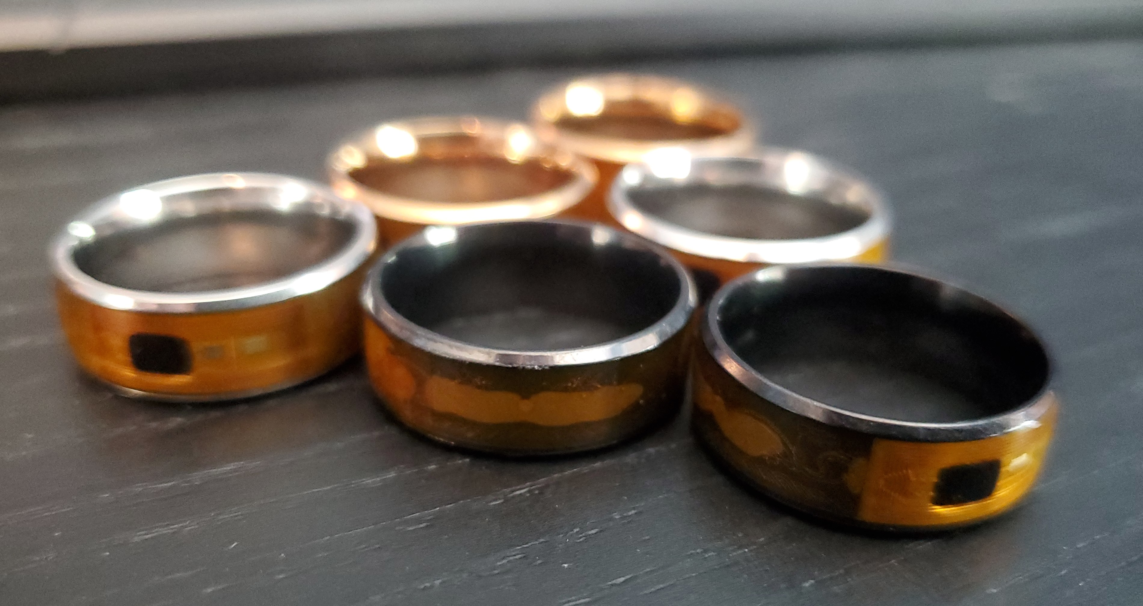
Much to my surprise, all of them worked(!), though their range is extremely short; you basically have to place the tag right up against the reader device in your phone for it to pick up the signal. Using the NFC Tools app, we can read off the attributes of the tags. The tag type is "Mifare Ultralight (Ultralight C)", as opposed to the "NTAG216" of the earlier ring (check out the datasheet from NXP), and it uses NFC Forum Type 2 data format, the same as before. As for memory, these ones only have 137 writable bytes (180 total), though none of the lock bits are set, so we can freely create new NDEF records on the device! I'm going to be a bit meta here and add a URL record to this very blog post: https://www.ecotner.com/blog/nfc-hacking. NFC Tools has a high-level utility for writing records that is a fair bit easier to use than specifying the bytes manually through the advanced commands utility, so I'll try that. After writing to the tag and manually inspecting the memory, we find the following:
| page | bytes | notes |
|---|---|---|
| x04 | 01:03:A0:0C | First 4 bytes of "lock control TLV" (see explanation below) |
| x05 | 34:03:21:D1 | Last byte of lock control TLV (0x34), beginning of NDEF message TLV header (0x03 = "NDEF message", 0x21 = "33 bytes of data"), and beginning of the first NDEF record (0xD1 = 0b11010001, meaning the MB, ME, and SR bits are set, and the TNF is "NFC WKT"). |
| x06 | 01:1D:55:02 | 0x01 = "record type is 1 byte", 0x1D = "payload is 29 bytes", 0x55 = "record type is U (URI)", 0x02 = "URI prefix is https://www |
| x07 | 65:63:6F:74 | "ecot" |
| x08 | 6E:65:72:2E | "ner." |
| x09 | 63:6F:6D:2F | "com/" |
| x0A | 62:6C:6F:67 | "blog" |
| x0B | 2F:6E:66:63 | "/nfc" |
| x0C | 2D:28:61:63 | "-hac" |
| x0D | 6B:69:6E:67 | "king" |
| x0E | FE:00:00:00 | 0xFE = "termination byte for TLV message", followed by null bytes |
We can see that there are actually 2 TLV blocks in memory. The second one is the one we just wrote with the URL to the blog, but the first one is a "lock control TLV", which we haven't encountered before. Why is that there? Looking at the other rings, they all appear to have the following data written to them by default starting at page 0x04:
page    data
------------
0x04    01:03:A0:0C
0x03    34:03:00:FE
(null bytes for rest of memory)
This is also composed of two TLV blocks; a lock control and an NDEF message (although 0x0300 indicates the message is of zero length). So I guess the lock control block is just there by default and when we write to the tag we're just overwriting the blank NDEF message block, leaving the first unchanged. If you're curious, the meaning of the lock control block is:
- 0x01: tag is of type "lock control"
- 0x03: length is 3 bytes (this is always true so is basically required)
- 0xA0: start position of the lock area, split into two nibbles (0xA = "start at page 0x0A", 0x0 = "offset of 0 bytes")
- 0x0C: size of lock area is 0x0C=12 bits
- 0x34: "page control" info; first nibble 0x3 = "2^3=16 bytes per page", second nibble 0x4 = "4 bytes (i.e. 1 page) locked per bit"
Final thoughts
This was a real deep-dive into the world of NFC; I had no idea I would be delving this far into the weeds when I first set out to hack that first ring. Even though the first ring couldn't be overwritten in the way that I wanted, it is very satisfying knowing at the actual firmware/protocol level how it all works and what kind of capabilities and limitations NFC technology has. Knowing how individual bits set on the tag can make or break the utility of the device is pretty cool.
At first I was pretty frustrated that I couldn't "wipe" the ring and reset the lock bits, but then I started thinking about the implications this could have, particularly on security. Some NFC tags have password protection capabilities, but many do not, and even so, passwords can be hacked. An NFC tag doesn't have any safety features like locking out after multiple failed attempts, 2FA/MFA, or other forms of verification. And because of limited memory on the tag, passwords need to be pretty short (on the NTAG216 the password is only 32 bits, meaning \(2^{32} = 4.3\times 10^9\) combinations); you could probably brute force hack one in a relatively short period of time by just trying different combinations over and over again. So it makes sense that someone would want to lock down a tag to prevent malicious actors from modifying it. For example, if you used NFC in a warehouse to log inventory transfers as you were loading goods onto a truck and someone was able to replace the codes on a tag that indicated the shipping destination, you could end up accidentally sending goods to the wrong customer. If someone replaced codes that indicated product SKU, you could end up putting items in places they don't belong and messing up how things are organized, or delivering the wrong product to a customer. Mistakes like those could be costly, especially if the error isn't caught quickly and multiple mistakes are made in sequence. Probably far better to ensure the tags can't be modified even if it means you have to replace them entirely rather than modifying them. And if the price of the rings I bought is any suggestion, the technology is incredibly cheap (a cursory look on digikey shows about $0.15/tag for the Mifare Ultralight when purchased in bulk), so replacements are a no-brainer.
Another point I found interesting is just how easy it was for me to read from or write to an NFC tag. Initially I thought I might need to get some piece of specialized equipment to view the raw data or overwrite it, but no, all you need is a modern smartphone! With apps like NFC Tools (which is free by the way) practically anyone can investigate the contents of an NFC tag and customize them as they see fit (subject to locking bits). Though I believe industry/logistics might benefit the most from NFC technology, everyday consumers can also take advantage of it too to easily share/stream data over short distances (recall that there is a message chunking capability in the NDEF protocol), or quickly interact with electronics (e.g. scanning your phone to gain entry to a secure area or read a link to a restauraunt menu or other informational data). And because the information transfer is bi-directional, it is vastly more useful than QR codes (which are already seeing a huge number of different use cases); you can leave messages or data on a passive device for other people to read rather than simply reading a static payload. Everyday people can start using this technology to make their lives easier in a multitude of ways, and I think we have only just scratched the surface of what's possible so far.
Perhaps the biggest thing I took away from this whole process though is a sense of gratitude to the people that took the time to develop the ISO 14443, NFC Forum and NDEF standards, as well as all the electronics engineers that designed the actual tags and reading devices, without which none of this technology would be possible. Most people don't even really know what NFC is or can be used for, but making it possible probably took thousands or maybe even millions of man-hours of effort involving many international collaborators and vendors.